
Here's what I have:
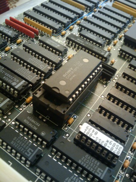
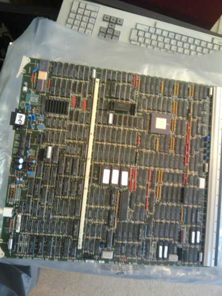
* The 4D/380 has an MC2 030-0117-010 rev A, with 32*8MB SIMMs installed.
* The 4D/440 has an MC2 030-0117-034 rev C, with 32*8MB SIMMs installed.
MC2's in storage:
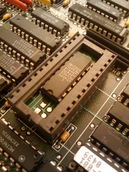
1 * 030-0117-034 rev B (with 32*2MB SIMMs installed).
2 * 030-0117-026 rev A.
1 * 030-0117-009 rev A.
So, my both MC2s with high density RAM are a newer rev. than yours. Unfortunately, this doesn't offer conclusive proof whether the older card is should support high density RAM.
* The 4D/380 has an MC2 030-0117-010 rev A, with 32*8MB SIMMs installed.
* The 4D/440 has an MC2 030-0117-034 rev C, with 32*8MB SIMMs installed.
MC2's in storage:
1 * 030-0117-034 rev B (with 32*2MB SIMMs installed).
2 * 030-0117-026 rev A.
1 * 030-0117-009 rev A.
So, my both MC2s with high density RAM are a newer rev. than yours. Unfortunately, this doesn't offer conclusive proof whether the older card is should support high density RAM.
_________________
Now this is a deep dark secret, so everybody keep it quiet

It turns out that when reset, the WD33C93 defaults to a SCSI ID of 0, and it was simpler to leave it that way... -- Dave Olson, in comp.sys.sgi
Currently in commercial service:


 (2x)
(2x)

In the museum: almost every MIPS/IRIX system.