The good news is that it is possible to remove the upper plastic surround from the main carrier assembly without doing irreparable damage:
Attachment:
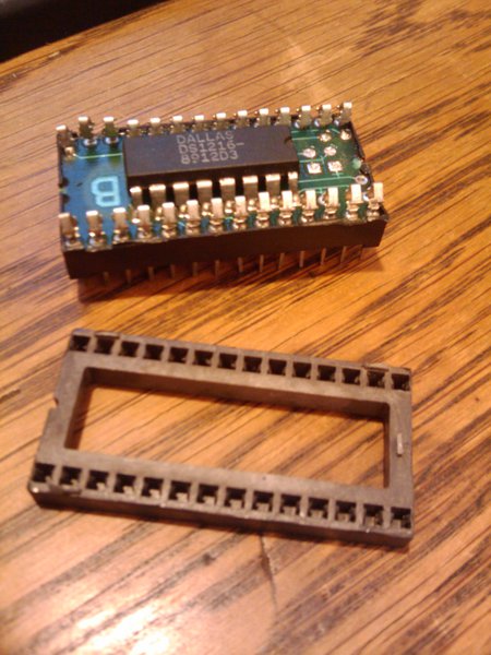 2010-01-29 21.38.38.jpg [ 526.72 KiB | Viewed 178 times ]
The bad news is that there's no single 'smoking gun' pin to cut and re-route....
rscottdrysdale wrote:
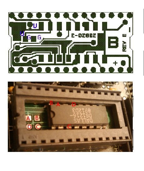
ok, looks like if the A,B,C,D labels on the chip pins correspond (check with an ohmmeter) to the A,B,C,D labels on the circuit board pads in your picture, then you can hopefully just cut the trace stub leading "up" from the A pad. the assumption is that battery + is wired to that pad underneath the carrier board, and cutting that trace will disconnect the battery from the whole circuit. use a SHARP exacto-type knife, being careful not to cut any other traces (or yourself).
Yes, that's how I verified that they were connected (an ohmmeter).
Okay, well, I've tried it. However, cutting pin 15 still left power to other pins. The highest voltage all along, even before the snip, was at pin 4 and did not correspond to A, B, C, or D. So I cut that one too. Well, several pins still have a potential difference between them and carrier GND, most notably 14. So, I *could* cut that too...but we're obviously getting into a situation where it's not a simple battery-to-pin connection I'd have to replicate -- it's a whole circuit of some sort, unknown at this point.
Attachment:
File comment:
the damage
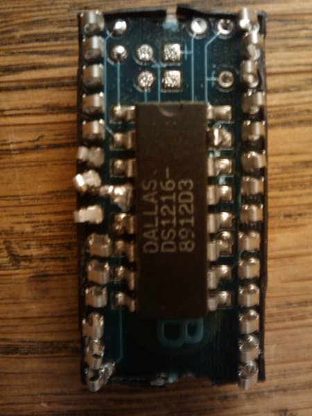 2010-01-29 23.16.14.jpg [ 479.22 KiB | Viewed 178 times ]
For reference, the magnitude of the potential differences was greatest at pin 4, then 15, then 14. This means that the battery was most likely to be applied with the least amount of intervening circuitry to pin 4, etc., in that order.
We may have to go back to the diode plan, since I can't see how to proceed here with three different voltages -- obviously the true battery + connection is obfuscated by/behind circuit board.